Designing a Low Latency 10G Ethernet Core - Part 3 (Low Latency Techniques)
![]() View the code on GitHub
View the code on GitHub
Links to the other parts in this series:
- Introduction
- Design Overview and Verification
- Low Latency Techniques (this post)
- Performance Measurement and Comparison
- Potential Improvements
Low Latency Techniques
This post describes some of the techniques used to reduce the latency of the Ethernet core:
- Custom Synchronous Gearbox
- PMA Buffer Bypass
- Slicing-by-N CRC Algorithm
- Minimal Buffering
The GTY latency values described here can be found in 69011 - UltraScale+ GTY Transceiver: TX and RX Latency Values - values for the 32-bit internal/32-bit interface width are used.
Custom Synchronous Gearbox
In digital logic, a gearbox is used for width conversion while maintaining a constant overall data rate. For example, a parallel to serial converter could be described as a gearbox, taking N bits every N cycles and outputting 1 bit every cycle.
For 10G Ethernet this becomes slightly more complex, and is derived from the 64b/66b encoding. Data in 10G Ethernet is formed into 66-bit frames, which includes 64-bits of ‘data’ and a 2-bit header. The header describes whether the frame is payload data only, or whether the data in the frame also contains control information. For example, in order to maintain clock recovery, frames are always transmitted at Ethernet Layer 1 regardless of whether data is being sent - these are IDLE control frames.
Because of this overhead, if the line rate of 10G Ethernet was precisely 10Gbps, the true data rate would actually be:
\[10 \cdot 64/66 = 9.696...Gbps\]To counter this, the line rate of 10G Ethernet is actually:
\[10 \cdot 66/64 = 10.3125Gbps\]Nice. Here comes the tricky bit - the interface to the GTY transceiver can be one of (16/20/32/40/64/80) bits wide - no multiples of 66. That means that at some point, the 66-bit frame must be width converted to (in our case) 32 bits while maintaining the same overall throughput. This can be done with an asynchronous or synchronous gearbox. An asynchronous gearbox is the simplest - 66 bits of data are written into a buffer every cycle at \(10312.5/66 = 156.25MHz\) and 64 bits of data are read out every cycle at \(10312.5/64 = \sim161.13MHz\). Crossing clock domains has an additional latency impact, and the asynchronous gearboxes in the GTY transceiver have a latency of about 30ns on transmit and receive.
The alternative is to place 66 bits of data into a buffer at ~161MHz but not every cycle - actually 32 of every 33 cycles. This maintains the overall throughput and means the gearbox can run on a single clock. In a 32-bit design, 32 bits of data + the 2 bit header are written in the first cycle, and the remaining 32 bits on the second at ~322MHz. This is referred to as the synchronous gearbox and Xilinx’s implementation in the GTYs has 6.2 to 12.4ns (2 to 4 cycles) of latency for TX and 3.1 to 9.4ns (1 to 3 cycles) latency for RX.
However, implementing a custom gearbox proved to reduce average latency by ~8.5ns (nearly 3 cycles) as shown in Figure 1. This is for two reasons:
- The latency of the GTY gearbox implies that the inputs and outputs to the gearbox are registered. The gearbox logic delay is less than a full cycle, so by integrating the gearbox into the PCS, other functionality (encoding/scrambling) can be performed in the same cycle.
- The gearbox in the GTY pauses for 2 consecutive cycles after 64 cycles, rather than pausing for a single cycle after 32 cycles. This adds a cycle to the maximum latency for transmit and receive. My assumption is that this method makes the alignment logic simpler on receive.
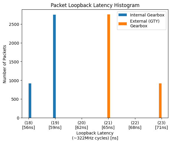
Figure 1: Internal vs External Gearbox Loopback Latency
Designing the custom gearbox was actually quite challenging, as it is almost impossible to debug visually with binary data. Instead, I built a model in Python which operated on strings, allowing me to visually confirm correct operation. This model was then integrated into a testbench as a ‘golden reference’ and used to verify operation with random input to the HDL. The trickiest aspect here was the receive alignment, so to verify correct operation a variable bit delay is implemented into the loopback mechanism of the main MAC/PCS UVM testbench, and the design is verified automatically under different scenarios with pytest.
Cycle | Slip | Data    | Header | Buf   |    Header Output     |   Data Output
Count |      | Valid   | Valid  | Index |                      |
---------------------------------------------------------------------------------------
32    |  0   | True    |   1    |   34  | ['46-D00', '46-D01'] | ['46-D02', '46-D03', '46-D04', '46-D05', ... '46-D32', '46-D33']
00    |  1   | True    |   0    |   00  | ['47-D00', '47-D01'] | ['46-D34', '46-D35', '46-D36', '46-D37', ... '47-H00', '47-H01']
00    |  0   | False   |   0    |   00  | ['47-D31', '47-D32'] | ['46-D33', '46-D34', '46-D35', '46-D36', ... '46-D63', '47-H00']
01    |  0   | True    |   1    |   32  | ['47-D31', '47-D32'] | ['47-D33', '47-D34', '47-D35', '47-D36', ... '47-D63', '48-H00']
02    |  1   | True    |   0    |   64  | ['48-D31', '48-D32'] | ['48-H01', '48-D00', '48-D01', '48-D02', ... '48-D29', '48-D30']
02    |  0   | True    |   0    |   64  | ['49-H00', '49-H01'] | ['48-D00', '48-D01', '48-D02', '48-D03', ... '48-D62', '48-D63']
03    |  0   | True    |   1    |   30  | ['49-H00', '49-H01'] | ['49-D00', '49-D01', '49-D02', '49-D03', ... '49-D30', '49-D31']
04    |  0   | True    |   0    |   62  | ['50-H00', '50-H01'] | ['49-D32', '49-D33', '49-D34', '49-D35', ... '49-D62', '49-D63']
05    |  0   | True    |   1    |   28  | ['50-H00', '50-H01'] | ['50-D00', '50-D01', '50-D02', '50-D03', ... '50-D30', '50-D31']
06    |  0   | True    |   0    |   60  | ['51-H00', '51-H01'] | ['50-D32', '50-D33', '50-D34', '50-D35', ... '50-D62', '50-D63']
07    |  0   | True    |   1    |   26  | ['51-H00', '51-H01'] | ['51-D00', '51-D01', '51-D02', '51-D03', ... '51-D30', '51-D31']
Figure 2: Gearbox Model Output Extract
Latency Saving (GTY Asynchronus vs Custom) = ~60ns
Latency Saving (GTY Synchronus vs Custom) = 8.5ns average
PMA Buffer Bypass
By default in Xilinx GTY transceivers, there are two clock domains - the PCS clock domain and PMA clock domain, shown for TX below. The PCS clock domain contains the PCS parallel clock and user-logic parallel clock, while the PMA clock domain contains the PMA parallel clock and serial clock.
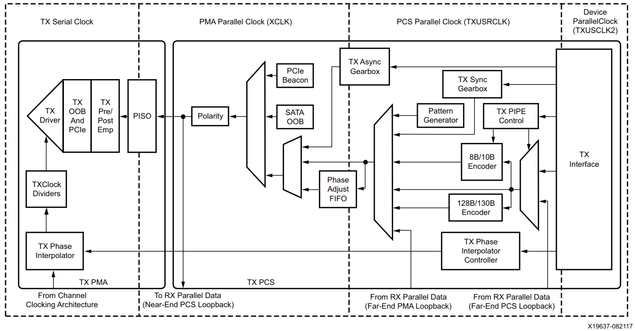
Figure 3: GTY TX Clock Domains (Ref 1: Figure 3-17)
By default, the two clock domains are not phase aligned, and a buffer is used to cross the domains when not using an asynchronous gearbox as discussed earlier. Unsurprisingly this comes at the cost of latency - 7.7 to 10.9ns on transmit and 13.2 to 17.1ns on receive. However, it is possible to phase align the two clock domains using the embedded phase alignment circuit. This was actually surprising easy to implement and only required configuration within the gtwizard IP.
Latency Saving = ~18 to 25ns
Minimal Buffering
Buffering and pipelining is the enemy of low latency operation. This sounds simple, but knowing where it could not be avoided was the most challenging aspect of the project. The design is right on the edge of passing timing for my device, to the point where I’m scared to change anything and rebuild. Pipelining not only eases the pressure on timing closure but makes processing the data easier, particularly when calculating the CRCs.
An example of this is when calculating the CRC on received packets. A typical MAC may buffer the whole packet, calculate the CRC and then only if it was correct give the packet to the user. A low latency MAC gives the data to the user as it is received to allow the user to start processing, while calculating the CRC on-the-go. A flag is then asserted at the end of the packet if the CRC was correct. In this design, the flag is asserted either on the last AXIS transfer of the packet or one cycle after, depending on how many bytes were in the packet. Delaying this further would ease the pressure on timing as the receive CRC chain is in the critical path.
Latency Saving = Tens to Hundreds of ns
Slicing-by-N CRC Algorithm
While delaying CRC calculation might be acceptable on receive, any delay in inserting the CRC for TX also delays the sending of the frame. Therefore it is necessary to update the CRC with 32 bits of data in a single cycle. At 322MHz, the naive bit-at-a-time approach is not viable. Luckily fast CRC algorithms are well studied, and one of the most common implementations is Sarwate’s algorithm, which uses an 8-bit, 256-entry lookup table which updates the CRC a byte-at-a-time. Unfortunately a 32-bit, 4-billion entry lookup table isn’t feasible on an FPGA, but Sarwate’s algorithm can be parallelised for multi-byte inputs with the “Slicing-by-8” algorithm described by Intel in “High Octane CRC Generation with the Intel Slicing-by-8 Algorithm” (original source no longer available) (Edit: Web Archive) . This design uses a Slicing-by-4 implementation, and it means no additional pipelining is required to calculate the CRC, however it is in the critical path for transmit and receive.
Latency Saving = ~3 to 6ns
Next Post - Performance Measurement and Comparison